
Featured image: Tesla
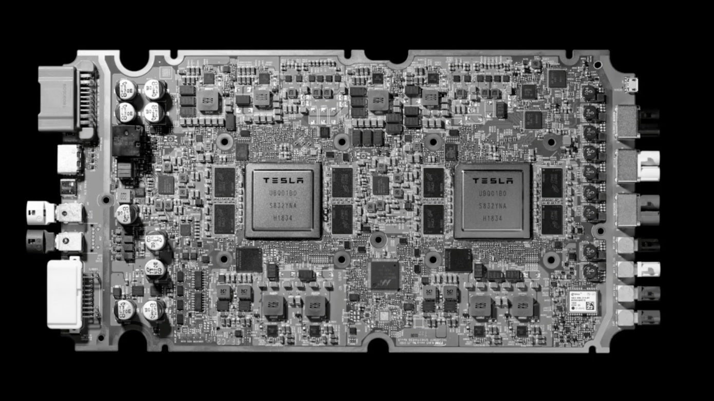
Electronics are currently installed in a large number of devices ranging from computers, automobiles, appliances, homes, and so on. Switching power supplies are commonly used to provide DC power within these electronics by performing voltage conversion, e.g., converting an input DC voltage to a lower DC or converting an input AC voltage to DC voltage. As an example, a Voltage Regulator Module (VRM) may be used to convert a voltage received from a battery or other DC source to a lower voltage for use by an Integrated Circuit (IC).
The requirement of high power for ICs, e.g., in excess of 500 watts, at relatively low voltages, e.g., less than one volt, creates problems for the VRM. The VRM must supply a relatively low DC voltage at many hundreds of amperes. Typically, VRMs are space constrained but must still include necessary components to produce clean power at a low voltage and with high current. The VRMs require substantial capacitance, inductance, and resistance to condition their output DC voltage, which typically requires a large number of lumped elements, e.g., capacitors, inductors, and resistors. It is difficult to include a large number of lumped elements in a small form factor device, e.g., a small foot print.
In the 'Packaged device having embedded array of components' patent application, Tesla tries to solve these difficulties.
Patent filing date January 6, 2020
Patent Publication Date July 9, 2020
The patent relates generally to electronics, and more specifically to the structure of packaged integrated circuits. It describes a structure having embedded array of components is described. An example structure includes an imbedded component array layer having an array of imbedded passive devices contained therein. The structure further includes an Integrated Fan-Out (InFO) layer residing adjacent a first surface of the imbedded component array layer having traces and vias formed therein. The structure further includes an insulator layer residing adjacent a second surface of the imbedded component array layer and electrically coupled to at least the InFO layer and vias passing through the imbedded component array layer and electrically coupled to some of the vias of the InFO layer.

FIG. 2 is a block schematic diagram illustrating a multiple circuit board high power VRM according to the present disclosure | Tesla patent
About the Author

Eva Fox
Eva Fox joined Tesmanian in 2019 to cover breaking news as an automotive journalist. The main topics that she covers are clean energy and electric vehicles. As a journalist, Eva is specialized in Tesla and topics related to the work and development of the company.


